
How to Calculate MIPI DSI Lane Count and Data Rate
Begin a MIPI DSI lane-rate calculation with active pixel payload, then prove that the packets fit the available transfer time. Resolution × refresh × transmitted bits per pixel ÷ data lanes gives a useful lower bound. It does not include every timing and protocol constraint needed for a working display.
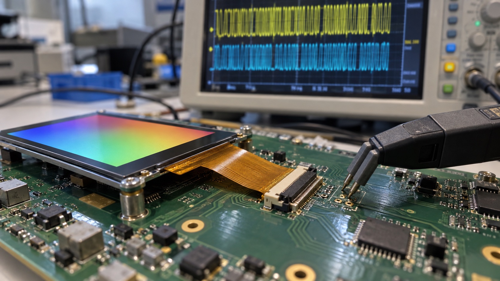
This guide covers uncompressed DSI over a conventional D-PHY link with a forwarded clock lane. C-PHY, compressed streams, and other PHY options require their own calculation rules. All numerical examples are illustrative; the hero is an AI-generated lab illustration.
Collect the Inputs Before Calculating
| Input | Why it matters |
|---|---|
| Active width and height | Number of image pixels |
| Wire pixel format | Actual transmitted bits, including packing |
| Required refresh or update rate | Number of images or regions per second |
| Supported data-lane counts | Common capability of host, panel, and board |
| Video or command mode | Determines the transfer schedule |
| Horizontal and vertical timing | Establishes line and frame deadlines |
| Allowed lane-rate range | Both minimum and maximum can matter |
| PHY transitions and clock behavior | Reduce usable transfer time or constrain operation |
The MIPI Alliance DSI overview distinguishes DSI’s D-PHY basis from the broader PHY options of DSI-2. Check the exact interface generation and device capabilities instead of borrowing a bandwidth formula from a different PHY.
For mode selection, use command mode vs video mode.
Step 1: Calculate the Active-Pixel Payload
For an uncompressed full image:
Payload_bits_per_second = Width × Height × Refresh_Hz × Wire_bpp
Payload_per_lane = Payload_bits_per_second / Number_of_data_lanes
For an illustrative 800 × 480 RGB888 display at 60 Hz:
Payload = 800 × 480 × 60 × 24
        = 552,960,000 bit/s = 552.96 Mbit/s
| Data lanes | Active-payload lower bound per lane |
|---|---|
| 1 | 552.96 Mbit/s |
| 2 | 276.48 Mbit/s |
| 4 | 138.24 Mbit/s |
The table shows division of payload, not three guaranteed valid configurations. A panel wired for two lanes may not support one or four. Even a supported lane count can fail if the calculated operating rate falls outside a host or receiver limit.
Step 2: Use the Wire Format, Not the Framebuffer Label
A 32-bit ARGB framebuffer can feed an RGB888 wire stream after the host handles alpha and format conversion. In that case, memory reads use four bytes per stored pixel while image payload uses three transmitted bytes per pixel.
The opposite mistake occurs with RGB666: a description of 18-bit color does not prove that its transport uses only 18 bits per pixel. Packed and loosely packed representations differ. Confirm the packet format selected at both ends and any pixel-group alignment.
Keep three quantities separate in the calculation sheet: stored bytes per pixel, wire bits per pixel, and panel color capability. They need not be numerically identical.
Step 3: Account for Video Timing
If the illustrative panel has Htotal = 1056, Vtotal = 525, and 60 Hz refresh, its pixel clock is 33.264 MHz. See the RGB timing calculation for the full derivation.
A common first-pass video estimate is:
Timing-based lane rate = Pixel_clock × Wire_bpp / Data_lanes
                      = 33.264 MHz × 24 / 2
                      = 399.168 Mbit/s per lane
This reserves a pixel-equivalent bit budget over the complete raster timing. It is not a statement that every blanking interval carries RGB pixels, nor is it proof that every packet configuration fits. DSI can represent timing with packets, blanking intervals, and permitted link-state transitions.
The host’s burst/non-burst behavior and receiver buffering decide how that budget can be used. ST’s DSI peripheral documentation describes the different clock constraints of burst and non-burst operation on its supported devices. Use such implementation guidance together with the panel’s timing limits.
Step 4: Check a Line-Time Budget
For the same example:
Line time = 1 / (525 × 60) = 31.746 µs
Active line payload = 800 × 3 = 2400 bytes
Suppose the proposed link uses two data lanes at 450 Mbit/s each. Ignoring overhead, the active-line payload occupies:
2400 × 8 / (2 × 450,000,000) = 21.333 µs
That leaves about 10.413 µs within the total line period before accounting for the chosen schedule. It is useful headroom, but not automatically usable low-power time: sync intervals, porch placement, packet headers and checks, lane alignment, entry/exit transitions, and host restrictions consume or constrain it.
Build the actual schedule with the host reference manual or its validated configuration tool. Include every packet type and transition the selected mode uses. Check each constrained interval, not only the frame-average bandwidth.
A fixed “add 20%” multiplier can screen options early, but it cannot replace this timing check. Conversely, blindly adding large overhead to an already conservative estimate may select an unsupported lane rate.
Step 5: Convert Bit Rate to the Correct Clock Domain
For a conventional D-PHY lane at 450 Mbit/s:
| Quantity | Value |
|---|---|
| Per-lane bit rate | 450 Mbit/s |
| Lane byte clock | 56.25 MHz |
| Forwarded DDR clock frequency | 225 MHz |
Do not multiply the byte clock by lane count when a register expects a per-lane byte-clock count. The host may also have separate escape, reference, and display-controller clocks.
A horizontal time expressed in pixel clocks is converted to byte-clock cycles using its actual duration. For example:
Interval_seconds = Pixel_clock_count / Pixel_clock_Hz
Byte_clock_cycles = Interval_seconds × Lane_byte_clock_Hz
The result may need rounding or satisfy additional encoding rules. Verify the resulting total line time after conversion; independently rounding several intervals can create a mismatch.
Command Mode: Calculate Transfer Time for the Update
For a compatible command-mode panel, compute the payload of the actual update region rather than assuming a full frame on every application tick.
An illustrative 200 × 100 RGB888 region contains 60,000 pixel bytes. On two 450 Mbit/s lanes, its ideal HS payload time is about 0.533 ms. Add address-setting commands, packet overhead, transfer setup, and any LP/HS transitions to obtain a usable deadline estimate.
This calculation does not apply unchanged if the transfer is sent through a low-power command path with different throughput. Verify the selected transaction mode and driver implementation.
Then compare the completed transfer with the panel’s TE or scan-position requirements. The bandwidth must fit the synchronization schedule, not merely the average update rate.
Choose the Lane Count and Validate the Board
Select a lane count only after confirming the module pinout, host capability, software support, and rate range. More lanes can reduce the required rate per lane, but add routing, connector, and PHY-power considerations. Fewer lanes at a higher rate can make signal integrity harder.
Validate the proposed configuration with static patterns and the intended animation workload. Check protocol error counters, host FIFO status, temperature behavior, and supply margin. Use appropriate high-speed probing; an unsuitable probe can disturb the link.
If the calculated mode does not display correctly, use the MIPI DSI debugging checklist to separate power, initialization, PHY, and packet-timing faults.
Retain the payload calculation, line schedule, selected PLL settings, achieved clocks, and measured results. A defensible lane-rate choice has both arithmetic and device-specific timing evidence behind it.
Frequently Asked Questions
How do I estimate the minimum MIPI DSI data rate per lane?
For uncompressed active pixels, multiply width by height, refresh rate, and transmitted bits per pixel, then divide by the number of data lanes. This is a payload lower bound, not a complete configured lane rate; add the constraints from packet scheduling, blanking, and physical-link transitions.
Does the DSI clock lane count as a data lane?
No. In the conventional forwarded-clock D-PHY arrangement covered here, pixel data is distributed across data lanes. The separate clock lane does not add pixel-payload capacity.
What is the difference between lane bit rate and lane byte clock?
Lane bit rate is the number of transmitted bits per second on one data lane. The corresponding byte-clock frequency is conventionally that rate divided by eight. In conventional DDR D-PHY operation, the forwarded clock frequency is half the lane bit rate. Check the host's terminology.
Is adding 20 percent overhead always enough for MIPI DSI?
No. A fixed percentage is only an early estimate. The supported video mode, packet layout, line timing, transitions, clock behavior, and receiver constraints determine whether the transfer fits.
Does RGB666 always use 18 bits per pixel on the wire?
No. Packed RGB666 carries 18 pixel bits in its packed representation, while loosely packed RGB666 uses three transmitted bytes per pixel. Use the actual DSI packet format, not only the panel's color-depth description.