
How to Read a TFT LCD Module Datasheet
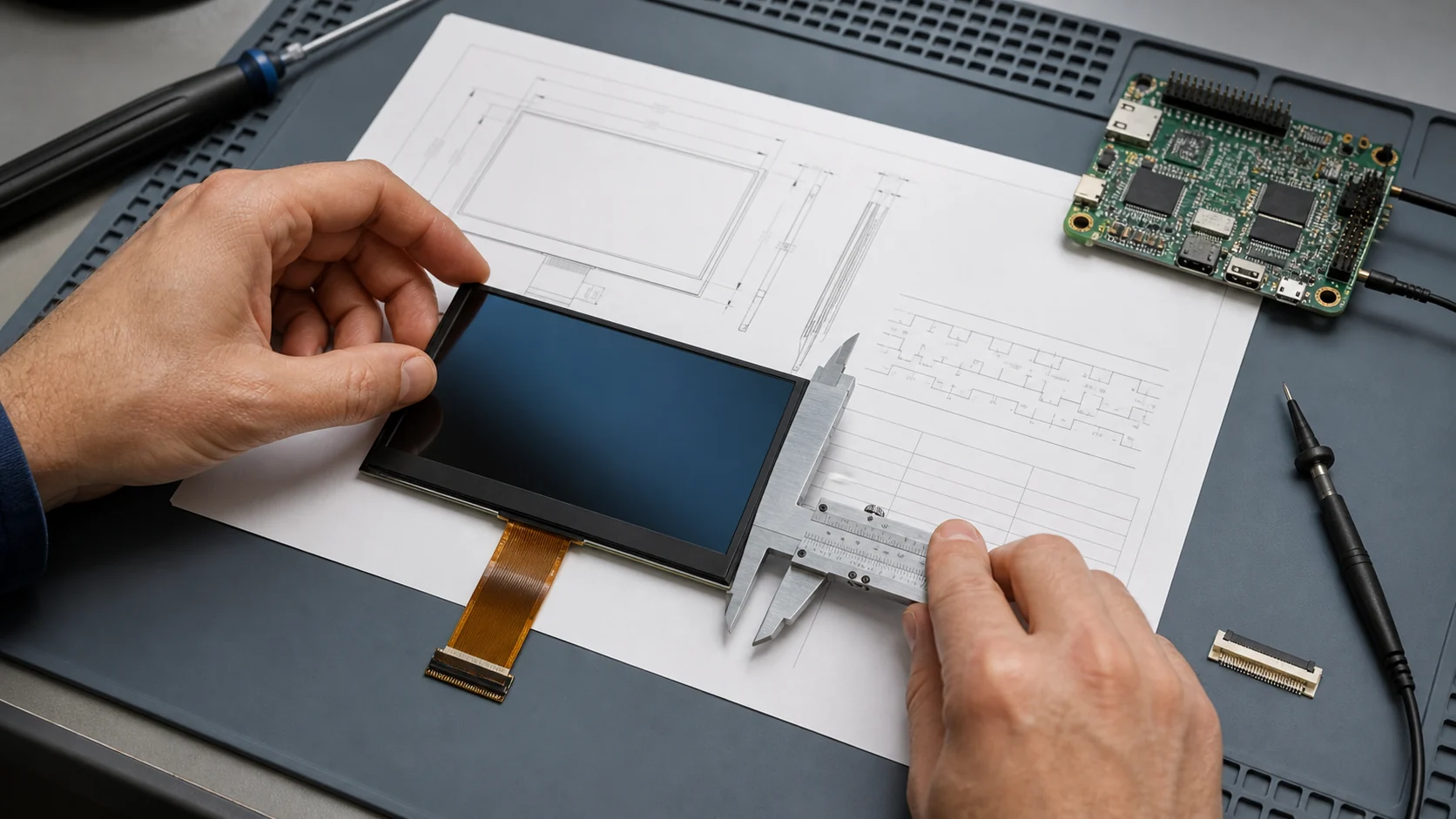
To read a TFT LCD module datasheet correctly, do not start with the diagonal size. Start with the exact part number and document revision, then review the mechanical drawing, active area, interface and pinout, voltage limits, timing, optical test conditions, temperature range, backlight life, and reliability notes. A module is suitable only when those sections agree with the enclosure, processor, power supply, user environment, and production requirements.
That is the short answer. The practical problem is that TFT datasheets mix three different kinds of information:
- Guaranteed limits, such as minimum and maximum supply voltage.
- Typical performance, such as nominal brightness or contrast under a stated test condition.
- Reference information, such as a recommended connector or a nominal mechanical dimension.
Treating all three as guarantees is one of the fastest ways to approve the wrong display.
This guide provides a repeatable engineering review process. It is designed for product developers, hardware engineers, mechanical engineers, buyers, and quality teams evaluating a standard or custom TFT LCD module. For broader product-level trade-offs, begin with how to choose a TFT display and use this article for the line-by-line datasheet review.
TFT LCD Datasheet Quick-Review Table
Use this table to decide where each specification belongs in the product design.
| Datasheet section | What it tells you | What to verify |
|---|---|---|
| Part number and revision | Exact module configuration and document version | Supplier quotation, sample label, revision history, product status |
| Mechanical drawing | Outline, thickness, active area, viewing area, FPC and tolerances | Enclosure opening, support surfaces, connector position, keep-out zones |
| Display mode and resolution | Pixel matrix, TN/IPS/VA behavior, orientation | UI layout, viewing direction, pixel order, mounting orientation |
| Interface and pinout | RGB, SPI, MCU, LVDS, MIPI DSI, control and touch signals | Host compatibility, voltage domains, connector, pin 1 and unused pins |
| Electrical characteristics | Supply voltage, logic thresholds and current | Regulator tolerance, level shifting, startup current, absolute maximums |
| Timing characteristics | Clock, porch, sync, setup and hold requirements | Display controller configuration and achievable refresh rate |
| Optical characteristics | Brightness, contrast, viewing angle, response and color | Minimum vs typical, backlight current, temperature and measurement method |
| Backlight section | LED topology, forward voltage, current and lifetime | Driver compliance, dimming, thermal load and expected brightness decay |
| Temperature and reliability | Operating/storage limits and qualification tests | Real use case, condensation, recovery criteria and test duration |
| Touch-panel section | Touch IC, interface, coordinates, glass and performance | Final cover lens, firmware, grounding, ESD, glove and water requirements |
1. Confirm the Exact Part Number and Revision
Display part numbers often encode the diagonal size, resolution, panel type, brightness option, touch option, temperature grade, and controller. A one-character suffix can identify a different FPC, viewing direction, backlight, or touch stack. Never review a “similar” family datasheet and assume it controls the sample on the bench.
Check four identifiers together:
- The complete part number on the purchase quotation.
- The label or laser marking on the physical module.
- The part number on the datasheet cover and mechanical drawing.
- The datasheet revision and date.
Revision history matters because a supplier may update the FPC layout, driver IC, optical values, drawing, or quality criteria without changing the marketing name. A public Newhaven 4.3-inch module specification, for example, records separate revisions for its mechanical drawing, driver IC, FPC layout, viewing angles, and chromaticity. That is a useful reminder to archive the approved PDF with the project instead of relying on a mutable download link.
Also check the product lifecycle. “Active,” “not recommended for new designs,” “last-time buy,” and “EOL” have very different sourcing implications. The datasheet describes technical behavior; it may not tell you whether the module will be available for the planned product lifetime.
2. Read the Mechanical Drawing Before the Specification Table
The drawing determines whether the module physically fits. The diagonal size alone does not define the outline, border width, active-area location, thickness, mounting support, or cable exit.
Module outline, active area, and viewing area
- Module outline is the maximum physical envelope of the supplied assembly.
- Active area (AA) is the region that contains addressable LCD pixels.
- Viewing area (VA) usually describes the intended visible opening or bezel aperture.
On a conventional LCD drawing, the VA is often slightly larger than the AA so the entire pixel region remains visible. Do not turn that observation into a universal rule: touch-panel drawings can use separate touch active-area and viewing-area labels, and supplier terminology is not perfectly standardized. Follow the labeled dimension, layer, and datum on the exact controlled drawing.
The difference is visible in real product documentation. Newhaven lists a 95.04 × 53.86 mm LCD active area and a 98.7 × 57.5 mm viewing area for one 4.3-inch module, while also specifying a larger module outline. These dimensions serve different mechanical decisions; none can replace the others.
For enclosure design, inspect:
- Overall width, height, and maximum thickness.
- Position of the AA relative to the outline datums.
- Recommended bezel opening and hidden border.
- FPC exit direction, length, bend radius, stiffener, and contact side.
- Connector pitch, mating direction, insertion depth, and pin 1 location.
- Components, solder joints, tapes, and driver ICs that need keep-out space.
- Frame tabs, mounting holes, alignment features, and allowed support areas.
- General tolerances plus any tighter local tolerance around the AA or FPC.
A dimension in parentheses may be a reference dimension rather than an inspection requirement. “Do not scale drawing” means exactly that: use the numerical dimensions, not measurements taken from a PDF screenshot.
If the module has a custom cover lens, compare the LCD AA, touch sensor, cover-lens viewing window, printed border, enclosure opening, and bonding tolerance in one stack-up. The touchscreen cover-lens guide explains the front-surface terms in more detail.
3. Decode Resolution, Pixel Format, and Orientation
A notation such as 480 × RGB × 272 usually means 480 horizontal pixels, each with red, green, and blue subpixels, by 272 vertical pixels. It does not mean 1,440 independently addressable horizontal pixels. Confirm whether the stated orientation is landscape or portrait and whether the driver can rotate the image in hardware.
Then check:
- Native resolution and aspect ratio.
- Pixel pitch and calculated active-area size.
- RGB or BGR color order.
- Supported input color depth, such as RGB565, RGB666, or RGB888.
- Whether the panel uses 6-bit color plus frame-rate control.
- Default scan direction and any mirror/rotation commands.
- Optimal viewing direction and gray-scale inversion direction for non-IPS panels.
The resolution and aspect-ratio guide covers the UI implications. For the datasheet review, the key question is compatibility: can the host produce the native resolution, color format, orientation, and update rate without expensive scaling or software conversion?
4. Separate the Interface, Driver IC, and Controller
These terms are often confused:
- The interface defines how the host sends commands or pixels: SPI, 8080/6800 MCU, parallel RGB, LVDS, or MIPI DSI.
- The driver IC generates the row and column drive waveforms required by the LCD glass.
- A display controller may include internal display RAM, timing generation, scaling, or a higher-level input such as HDMI.
A module with a driver IC does not automatically have a framebuffer. A raw RGB panel usually expects a continuous pixel stream with a valid pixel clock and synchronization. A controller-based SPI or MCU display often stores pixels in internal GRAM after commands and image data are written. This difference affects processor choice, memory bandwidth, pin count, software, and power.
For MIPI DSI, confirm lane count, supported data rate, command or video mode, pixel format, PHY requirements, and initialization commands. The MIPI Alliance defines DSI as a high-speed link between a host processor and display module; the module datasheet still has to specify the configuration that the particular panel accepts.
If the interface decision is still open, compare MIPI, LVDS, and RGB before selecting the module. If the processor has already been chosen, use the microcontroller and SBC matching guide to check host-side support.
5. Audit Every Pin and Voltage Domain
Do not stop after matching signal names. Build a pin-by-pin table that includes pin number, symbol, direction, voltage domain, reset state, pull resistor, host connection, and PCB net name.
Pay special attention to:
- Logic supply (
VDD,VCC,IOVCC, or similar). - Analog LCD rails when exposed (
AVDD,VGH,VGL,VCOM). - Input-high and input-low thresholds, not just nominal supply voltage.
- Reset polarity and minimum reset-pulse width.
- Chip select, data/command, display enable, tearing-effect, and standby pins.
- Pins marked
NC, reserved, or “do not connect.” - Backlight anode/cathode arrangement and LED string count.
- Touch-controller power, I2C/SPI lines, interrupt, reset, and I2C address.
“3.3 V module” can hide several requirements. The logic may accept 3.3 V while the series LED backlight needs a boosted voltage above 15 V. A public Winstar 2.86-inch specification illustrates this separation: it gives one range for the interface supply and a much higher forward-voltage range for the LED string.
Drive the backlight with regulated current, not an assumed fixed voltage. Forward voltage varies with temperature and production. The backlight driver guide covers current regulation and common topologies.
6. Distinguish Absolute Maximums from Operating Conditions
The absolute maximum ratings are damage boundaries, not design targets. Normal operation should remain inside the recommended range with margin for regulator tolerance, ripple, startup overshoot, temperature, and component variation.
Read each row across, including the condition column:
Minis the lowest guaranteed or permitted value under the stated condition.Typis a nominal value, generally not a production guarantee by itself.Maxis the highest guaranteed or permitted value under the stated condition.- The test condition explains when those numbers apply.
For power budgeting, do not use only typical logic current. Check maximum current, backlight current, touch current, inrush, sleep current, and any condition that changes with image content or clock rate. For signal integrity, compare the display’s input thresholds with the host’s guaranteed output levels across both devices’ voltage and temperature ranges.
7. Translate the Timing Table into Host Settings
Timing values are functional requirements, not optional tuning suggestions. For a parallel RGB panel, the horizontal total is normally:
Htotal = Hactive + Hsync + Hback porch + Hfront porch
The vertical total is:
Vtotal = Vactive + Vsync + Vback porch + Vfront porch
The approximate refresh rate is:
Refresh rate = Pixel clock / (Htotal × Vtotal)
Use one internally consistent set of min/typ/max values. Do not combine the minimum total with an unrelated maximum porch just because both appear in the table. Start with the supplier’s typical timing, confirm clock polarity and data sampling edge, and then validate the permitted range on hardware.
Also check:
- HSYNC, VSYNC, DE, and pixel-clock polarity.
- Sync mode versus DE-only mode.
- Data setup and hold time.
- Minimum reset width and delay before sending data.
- Power-on and power-off sequence.
- Backlight enable delay relative to valid image data.
For SPI or MCU interfaces, timing includes serial clock limits, chip-select setup, write/read cycles, command delays, and the initialization sequence. For MIPI DSI, it includes lane rate, low-power/high-speed transitions, packet format, escape clock, mode, and panel-specific commands. A working connector does not prove a working protocol.
8. Read Optical Specifications with Their Test Conditions
Brightness, contrast, viewing angle, color, and response time are only meaningful with the conditions used to measure them.
Luminance and contrast
LCD luminance is usually stated in cd/m², also called nits. Check whether the number is minimum or typical and note the backlight current, temperature, measurement point, and whether a touch panel or cover lens is included. A “780 cd/m² typical” panel measured at a specified LED current is not a promise that every assembled product will deliver 780 nits through its final touch-and-cover stack.
Contrast ratio is also measured under controlled conditions. Ambient reflections, an air gap, fingerprints, a glossy cover lens, and off-axis viewing can dominate real-world readability. High brightness alone does not guarantee sunlight readability.
Viewing angle, response, and color
Viewing angle is often defined at a contrast-ratio threshold, such as CR ≥ 10. Confirm the coordinate convention and whether values are listed as top/bottom/left/right. A single “6 o’clock view” entry identifies the preferred viewing direction; it is not equivalent to a four-direction IPS viewing-angle specification.
Response time may be reported as rise plus fall time at room temperature. LCD response normally slows at low temperature, so a room-temperature typical value cannot prove cold-start UI performance. Chromaticity coordinates describe measured primary and white points, but wide min/max tolerances may still allow visible unit-to-unit differences.
For products that need consistent units, define incoming and production measurement methods rather than relying only on a headline typical value. The brightness calibration guide explains how to establish repeatable measurement conditions.
9. Interpret Temperature, Lifetime, and Reliability Carefully
Operating temperature is the range in which the powered module is intended to function. Storage temperature is the unpowered survival range. Neither line guarantees constant optical performance across the full range.
At temperature extremes, validate:
- Cold-start response time and ghosting.
- High-temperature contrast, color, and black-state behavior.
- Backlight output and LED driver margin.
- Touch sensitivity and controller recovery.
- Condensation during transitions.
- Adhesive, polarizer, FPC, and cover-lens behavior.
Backlight life is commonly defined as the time until brightness falls to a stated fraction of its initial value under a specified LED current and ambient temperature. Confirm whether the number is minimum or typical, what end-of-life criterion is used, and whether thermal conditions in the final enclosure are comparable. It is not the same as guaranteed module service life.
Reliability tables may list high/low-temperature storage, powered operation, humidity, thermal shock, vibration, or ESD. The Newhaven example datasheet includes specific durations and recovery notes for these tests. Passing a short supplier qualification test does not mean the product is certified for every industry or will survive the customer’s complete mission profile. Use the table as evidence of module screening, then build a product-level validation plan.
10. Treat Touch as a Separate Subsystem
A TFT module with PCAP may contain an LCD, touch sensor, touch controller, cover lens, bonding adhesive, and two electrical interfaces. Read the LCD and touch sections independently before reviewing the complete stack.
Confirm the touch-controller part number or approved equivalent, firmware version, I2C address, supply, reset, interrupt behavior, coordinate resolution, number of touch points, report rate, and supported cover thickness. Then validate the final stack with the real enclosure, grounding, display noise, charger, gloves, water, and expected temperature range.
If the supplier writes “controller IC or equivalent,” ask what changes are allowed without approval. A controller substitution can affect firmware, device ID, tuning parameters, interrupt behavior, emissions, and test results even if the FPC pinout remains unchanged. For the underlying touch architecture, see capacitive touch-panel basics.
A Worked Datasheet Review Example
Suppose a candidate module is described as a 4.3-inch, 480 × 272, 24-bit RGB TFT with 3.3 V logic, LED backlight, and optional touch. A weak review says, “The size and voltage match.” A design review converts every field into an action:
| Datasheet value | Engineering interpretation | Required action |
|---|---|---|
| 4.3-inch diagonal | Marketing size, not enclosure size | Use outline, AA, VA, and tolerances from the drawing |
| 480 × RGB × 272 | Native pixel matrix with RGB subpixels | Confirm framebuffer size, pixel order, aspect ratio and UI assets |
| 24-bit RGB | Continuous parallel video interface | Confirm host pins, pixel clock, porch values and polarity |
| 3.3 V logic | Nominal logic rail | Verify min/max supply and VIH/VIL against the host |
| LED backlight | Separate power load | Select a constant-current driver from Vf and current limits |
| Typical luminance | Nominal result at a stated current | Request a controlled minimum if brightness is critical |
| Wide temperature | A range, not constant performance | Test cold response, hot contrast, touch and thermal margin |
| Optional touch | Separate sensor/controller configuration | Freeze controller, firmware, glass and coordinate requirements |
This translation step is where a datasheet becomes an engineering specification.
Questions to Send the Display Supplier
Before design freeze, ask for written answers to the following:
- Is this the latest controlled datasheet and drawing revision?
- What is the current product status and expected supply lifetime?
- Which specifications are guaranteed minimums in production?
- Does the quoted module include the touch panel, cover lens, bonding, and connector?
- Are the LCD and touch driver ICs fixed, or can equivalents be substituted?
- Which initialization code revision matches the sample?
- Are the power sequence and backlight delay mandatory?
- What are the pixel order, scan direction, and timing polarities?
- What connector part number and contact orientation are recommended?
- What cosmetic and pixel-defect acceptance criteria apply?
- How is luminance measured, and is a minimum value available?
- What does the backlight-life number mean, and under which current and temperature?
- Which reliability tests were run, on how many samples, and with what pass criteria?
- What PCN notice period applies to the panel, IC, FPC, backlight, and touch firmware?
- Can the supplier provide a signed specification for the production configuration?
Common TFT Datasheet Mistakes
Avoid these recurring errors:
- Selecting by diagonal size and resolution alone.
- Using a typical optical value as a guaranteed minimum.
- Confusing active area with the enclosure opening.
- Ignoring the FPC contact side or connector mating direction.
- Assuming logic voltage can power the LED backlight directly.
- Treating a driver IC as a framebuffer controller.
- Copying typical porch values without checking clock polarity and totals.
- Using storage temperature as proof of powered operation.
- Treating a qualification-test duration as expected field life.
- Accepting “or equivalent” components without a change-control agreement.
Ten-Minute TFT Datasheet Preselection Checklist
Before requesting samples, confirm all of these items:
- Exact part number, revision, and product status match the quotation.
- Module outline, maximum thickness, AA, VA, FPC, and connector fit the enclosure.
- Native resolution, orientation, color order, and viewing direction fit the UI.
- The host supports the interface, lane/pin count, driver, and initialization method.
- All supply and I/O voltage ranges are compatible with adequate margin.
- Backlight voltage, current, dimming, power, and thermal load are supported.
- Timing values can be generated by the chosen processor or bridge.
- Minimum optical performance is defined for the final touch/cover configuration.
- Operating temperature and validation tests match the real environment.
- Touch IC, firmware, glass stack, quality limits, PCN, and lifecycle are controlled.
Passing this checklist only qualifies the module for sampling. Final approval still requires measurement and functional testing with the actual processor, PCB, enclosure, power supply, cover lens, firmware, and environmental conditions.
Final Recommendation
Read a TFT LCD datasheet as a set of interfaces between teams. The drawing belongs in the mechanical stack-up; the pinout and electrical tables belong in the schematic review; timing belongs in the display-controller configuration; optical limits belong in the product requirement; temperature and reliability belong in the validation plan; lifecycle and change control belong in the supply agreement.
The best display is not the one with the most impressive typical value. It is the one whose controlled limits can be translated into a product that fits, starts reliably, remains readable, survives its environment, and can be built consistently.
Technical sources used
- Newhaven Display: NHD-4.3-480272EF-ASXN#-T specification — example of revision history, drawing, pinout, electrical/optical limits, timing, sequencing, and qualification tests.
- Winstar Display: WFN0286A2S0WADNA000 specification — example of general specifications, separate voltage domains, LED conditions, and interface pin definitions.
- MIPI Alliance: MIPI DSI — primary definition and capabilities of the MIPI Display Serial Interface.
These documents are cited as examples of datasheet structure, not as universal limits or product endorsements. Always use the current supplier-approved revision for the exact module being designed in.
Frequently Asked Questions
What should I check first in a TFT LCD datasheet?
Confirm the exact part number and datasheet revision first. Then check the mechanical outline, active area, interface, supply and I/O voltages, timing limits, brightness conditions, operating temperature, and product status before comparing headline specifications.
What is the difference between active area and viewing area?
The active area is the pixel-producing region of the LCD. The viewing area is the opening through which the display is intended to be seen. The viewing area is often larger than the active area on an LCD drawing, but terminology can differ between LCD and touch-panel drawings, so always follow the labeled dimensions on the exact drawing.
Does a typical brightness value guarantee every production module?
No. A typical value describes a nominal result under stated test conditions; it is not normally a guaranteed production minimum. If minimum luminance matters, put an agreed minimum value, test current, temperature, measurement geometry, and aging condition into the controlled specification.
Is storage temperature the same as operating temperature?
No. Storage temperature applies to an unpowered module and does not guarantee that the LCD will display correctly at that temperature. Operating temperature defines the powered range, but response time, contrast, color, and backlight output can still vary within it.
Can two TFT modules with the same size and resolution be drop-in replacements?
Not necessarily. They can differ in outline, active-area position, FPC location, pinout, voltage levels, pixel order, timing, driver IC, initialization sequence, backlight load, viewing direction, touch controller, and quality criteria. A line-by-line comparison and sample validation are required.