MIPI DSI Display Not Working: A Debug Checklist
When a MIPI DSI display does not work, debug it in layers: confirm the exact panel and DSI configuration, verify power/reset, prove low-power command communication, then enable high-speed video and inspect host/PHY error registers. Only after those checks should you tune lane rate, packet timing, clock mode, or D-PHY parameters.
MIPI DSI combines panel-specific commands, packet protocol, video timing, and a high-speed physical layer. A white or black screen can be produced by any one of those layers, so random register changes are inefficient and can hide the original failure.
Record the Known Configuration
Before probing, write down:
- Exact module part number and revision.
- Display driver IC and approved initialization table.
- Number of connected data lanes.
- DSI/DSI-2 host and D-PHY implementation.
- Command mode or video mode.
- Burst or non-burst video type.
- Pixel format and bits per pixel.
- Resolution, refresh rate, and porch/sync values.
- HS lane rate, escape clock, and reference clock.
- Continuous or non-continuous clock mode.
- Virtual channel and expected DCS reads.
Use the TFT LCD datasheet guide to verify that the module, sample label, quotation, drawing, and init code refer to the same variant.
MIPI DSI Failure Matrix
| Symptom | Likely layer | First evidence to collect |
|---|---|---|
| No current change, no backlight | Power/control | Rails, enables, backlight path |
| Backlight on, white screen | Init, video, panel power | DCS response, reset, video errors |
| DCS reads fail | LP state, wiring, reset, I/O level | LP lane states and host status |
| DCS works, no video | HS clock/data, mode, timing | PHY/video error registers |
| Image unstable or corrupted | Lane rate, SI, packet timing | CRC/ECC/SoT errors, clock measurement |
| Wrong colors | Pixel format, packing, panel order | Solid RGB patterns and format registers |
| Works only with continuous clock | Panel clock dependency | Clock-mode configuration |
| Works at low lane rate only | PHY/SI/timing margin | Error count versus rate |
For a generic white field on other interfaces, see TFT LCD white-screen troubleshooting. For corrupted images, see TFT LCD lines and artifacts.
Step 1: Verify the Module Is Electrically Ready
Measure every required rail at the display connector. Depending on the module, these may include logic I/O, analog panel, touch, and backlight supplies. Confirm the required sequence, reset polarity, minimum pulse width, enable pins, and delays.
Capture startup with an oscilloscope. A static multimeter value cannot reveal a rail that rises out of order or dips when the DSI stream starts.
Keep the backlight off until the panel has valid image data when the supplier recommends it. Backlight state does not prove DSI activity.
Step 2: Inspect Lane Wiring and Configuration
Compare the schematic with both host and module pin tables:
- Clock pair polarity and data-pair polarity.
- Lane 0 through lane N mapping.
- Connected lane count versus software configuration.
- Connector pin numbering and FPC contact side.
- Differential pair continuity and absence of shorts.
- I/O supply compatibility for low-power signaling.
- Ground/reference pins around the link.
Some devices support lane or polarity remapping; others do not. Enable remapping only when every device in the path documents it.
Inspect connector insertion, FPC strain, and any bridge IC between the host and panel. The FPC layout and pin-mapping guide covers mechanical and routing checks.
Step 3: Prove Low-Power Command Communication
Before video, use low-power mode to send a minimal panel startup and read a known register when supported.
Typical sequence elements include:
- Hardware reset and required delay.
- Software reset if required.
- Read display ID/status/power mode.
- Manufacturer-specific unlock and configuration commands.
- Pixel-format, orientation, porch, power, and gamma settings.
- Sleep-out command and mandatory delay.
- Display-on command.
Log the packet type, command byte, payload, return status, and host error flags. A transmitted command is not proof that the panel received it.
If reads fail, investigate reset, LP states, virtual channel, BTA/read configuration, packet data type, I/O supply, and physical wiring before enabling video.
Step 4: Validate the Initialization Table
Panel initialization is often vendor-specific even when DCS commands are used. Confirm:
- Driver IC and silicon revision.
- Supplier-approved sequence for the exact glass/module.
- Command order and delays.
- Page/bank unlock commands.
- Generic versus DCS packet type.
- Short versus long write.
- Pixel format and lane configuration.
- Sleep-out/display-on order.
Beware of copied device-tree or bootloader sequences for a visually similar panel. A module can share resolution and connector yet require different power, gamma, porch, or gate settings.
Step 5: Calculate Lane Rate and Pixel Throughput
Start with the active pixel payload:
Active bit rate = width × height × refresh rate × bits per pixel
Then add blanking and protocol overhead according to video mode and host implementation. Per-lane rate is total link rate divided by the number of data lanes, with appropriate overhead margin.
Check three boundaries:
- Host/D-PHY supported lane-rate range.
- Panel/D-PHY supported lane-rate range.
- Board/FPC signal-integrity capability.
Do not set lane rate solely from active pixels. Blanking packets, sync events/pulses, headers, ECC, CRC, and transitions consume link time.
Step 6: Match Host and Panel Video Modes
Confirm that both sides use the same mode:
- Command mode versus video mode.
- Burst versus non-burst sync-pulse or sync-event mode.
- Continuous versus non-continuous clock.
- Number of lanes.
- Pixel data type and loosely packed behavior.
- Virtual channel.
- Horizontal/vertical active and blanking values.
A panel that depends on the DSI clock as an internal timing source may require continuous clock during initialization or operation. A host configured to stop the clock in blanking can therefore show no image even though some commands work.
Step 7: Check All Clocks
Verify:
- Panel reference/input clock if separate.
- Host pixel clock.
- D-PHY HS bit clock.
- Escape/LP clock.
- PLL lock and divider calculations.
Confirm units. MHz, Mbps per lane, DDR clock frequency, byte clock, and pixel clock are related but not interchangeable.
Read back programmed dividers and status rather than trusting configuration-tool output. A rounded PLL solution may produce a lane rate outside the panel tolerance.
Step 8: Read Error Registers Before Clearing Them
Host and PHY status can report:
- Start-of-transmission (SoT) and sync errors.
- Escape entry or LP transmission errors.
- ECC single/multi-bit errors.
- CRC errors.
- False control or contention.
- FIFO overflow/underflow.
- PLL unlock or PHY lock failure.
- Packet-size/timing errors.
Record raw values after reset, after initialization, after starting video, and after the visible failure. Clear flags only between controlled tests.
Error patterns guide the next step. LP errors keep attention on command state and wiring; CRC/ECC/SoT errors during video point toward PHY timing or signal integrity; FIFO underflow points toward host bandwidth or pipeline setup.
Step 9: Inspect LP-to-HS Transitions and Clock Mode
Some failures occur only at state transitions. Check whether the host periodically returns lanes to LP state as expected and whether blanking-low-power behavior matches the panel.
Review D-PHY parameters such as prepare, zero, trail, exit, settle, and skip using the device documentation. Avoid arbitrary tuning: each parameter has a defined relationship to lane rate and receiver behavior.
If lowering the lane rate within both devices’ supported ranges removes errors, the link has a margin problem. The final fix may involve timing, stack-up, pair matching, impedance, connector, return path, or bridge configuration.
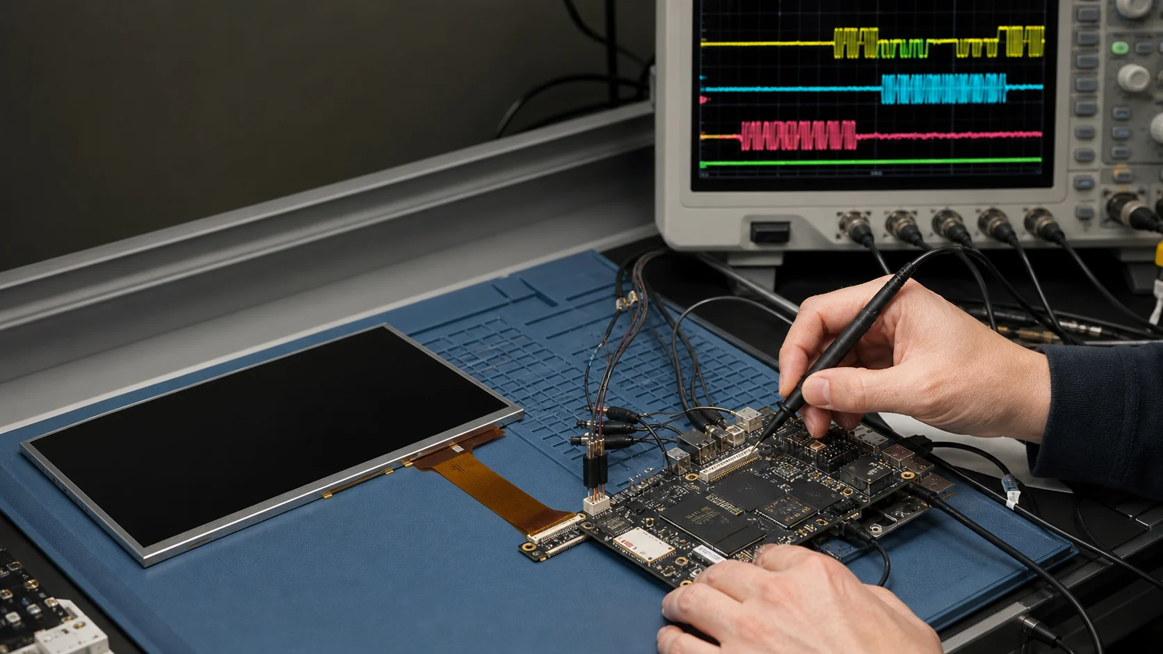
Step 10: Measure the Physical Layer Carefully
Begin with non-invasive evidence: error registers, PLL/PHY state, current consumption, and low-power pin levels. High-speed D-PHY measurement requires suitable differential probes, bandwidth, fixtures, and an understanding of the test point’s loading.
Check board design for:
- Controlled differential impedance.
- Pair length matching and limited skew.
- Continuous reference plane.
- Few vias and minimal stubs.
- Correct connector footprint and FPC orientation.
- Separation from noisy switch nodes and clocks.
- Appropriate ESD protection with low capacitance.
Do not probe a high-speed pair with long single-ended ground leads and interpret the resulting ringing as receiver behavior.
Step 11: Simplify the Video Path
Use the most conservative known-good configuration:
- Lower resolution or refresh rate if supported.
- Solid color bars generated near the display controller.
- One layer/plane with no scaling or compression.
- Fixed pixel format.
- Supplier typical timing.
- Minimal init sequence with verbose error logging.
Disable camera, GPU overlays, and unrelated high-bandwidth clients. If the display starts, add complexity one element at a time.
Step 12: Compare Bootloader and OS Behavior
If the panel works in a bootloader but fails in the OS, compare:
- Power regulator and GPIO ownership.
- Reset timing.
- Initialization commands.
- Clock tree and assigned rates.
- Device-tree lane/mode/timing properties.
- Runtime power management.
- Bridge and panel driver attach order.
If it fails in the bootloader but works later, the OS may be correcting a missing rail, command, delay, or clock. Capture both sequences rather than treating the working phase as unexplained.
Common MIPI DSI Debugging Mistakes
- Enabling video before proving LP commands.
- Copying an init table from a similar panel.
- Confusing pixel clock, byte clock, and lane bit rate.
- Ignoring error registers and tuning PHY blindly.
- Assuming lane/polarity swaps are universally supported.
- Measuring only at the host side of the connector.
- Starting with a complex compositor or GPU pipeline.
- Clearing errors before logging the failure state.
Bring-Up Checklist
- Exact module, driver IC, init revision, and lane count confirmed.
- Power, reset, enable, and delays measured at the FPC.
- LP command write and at least one expected status read confirmed.
- Pixel format, virtual channel, and panel mode match.
- Pixel, escape, and HS clocks calculated and measured/verified.
- Host and panel agree on video type and clock mode.
- Error registers logged at each bring-up stage.
- Conservative color-bar video works before full graphics.
- Differential routing, connector, and FPC checked.
- Cold, warm, sleep/wake, and repeated-reset tests pass.
Engineering References
- MIPI Alliance: MIPI Display Serial Interface (DSI) — primary overview of the host-to-display interface, D-PHY use, low power, performance, and EMI goals.
- NXP AN13573: i.MX 8/RT MIPI DSI/CSI-2 — detailed DSI checks for initialization, clocks, modes, LP/HS communication, packet timing, and error registers.
Use the current specifications and errata for the exact host, PHY, bridge, and panel. DSI register names and timing controls vary between implementations.
Frequently Asked Questions
Why is my MIPI DSI display black or white?
Common causes are incorrect panel power or reset, missing low-power initialization commands, mismatched lane count or video mode, wrong pixel format or timing, absent high-speed clock/data, incorrect D-PHY settings, or a panel-specific initialization table that does not match the module revision.
What should I check first on a MIPI DSI display?
Verify the exact panel variant, module power rails, reset and enable sequence, then confirm that low-power DCS commands receive expected responses before enabling the high-speed video stream. Read host and PHY error registers before changing timing parameters.
Can MIPI DSI lanes be swapped?
Lane mapping and polarity support depend on the host, bridge, and panel. Do not assume arbitrary lane or polarity swapping is allowed. Compare the schematic and device capabilities, and confirm that configured lane count matches the connected module.
Why do DCS commands work but video does not appear?
Low-power command communication and high-speed video use different operating states. Working DCS reads do not prove that lane rate, clock mode, video packet timing, pixel format, blanking, or high-speed D-PHY levels are correct.
Should I probe MIPI DSI lanes with a normal oscilloscope probe?
A normal single-ended probe can load and distort the high-speed differential link and may not show compliance-level behavior. Start with controller error registers and low-speed state checks; use appropriate high-bandwidth differential probing and a suitable fixture when physical-layer measurement is required.