
Vertical Lines, Horizontal Lines, and Artifacts on TFT LCDs
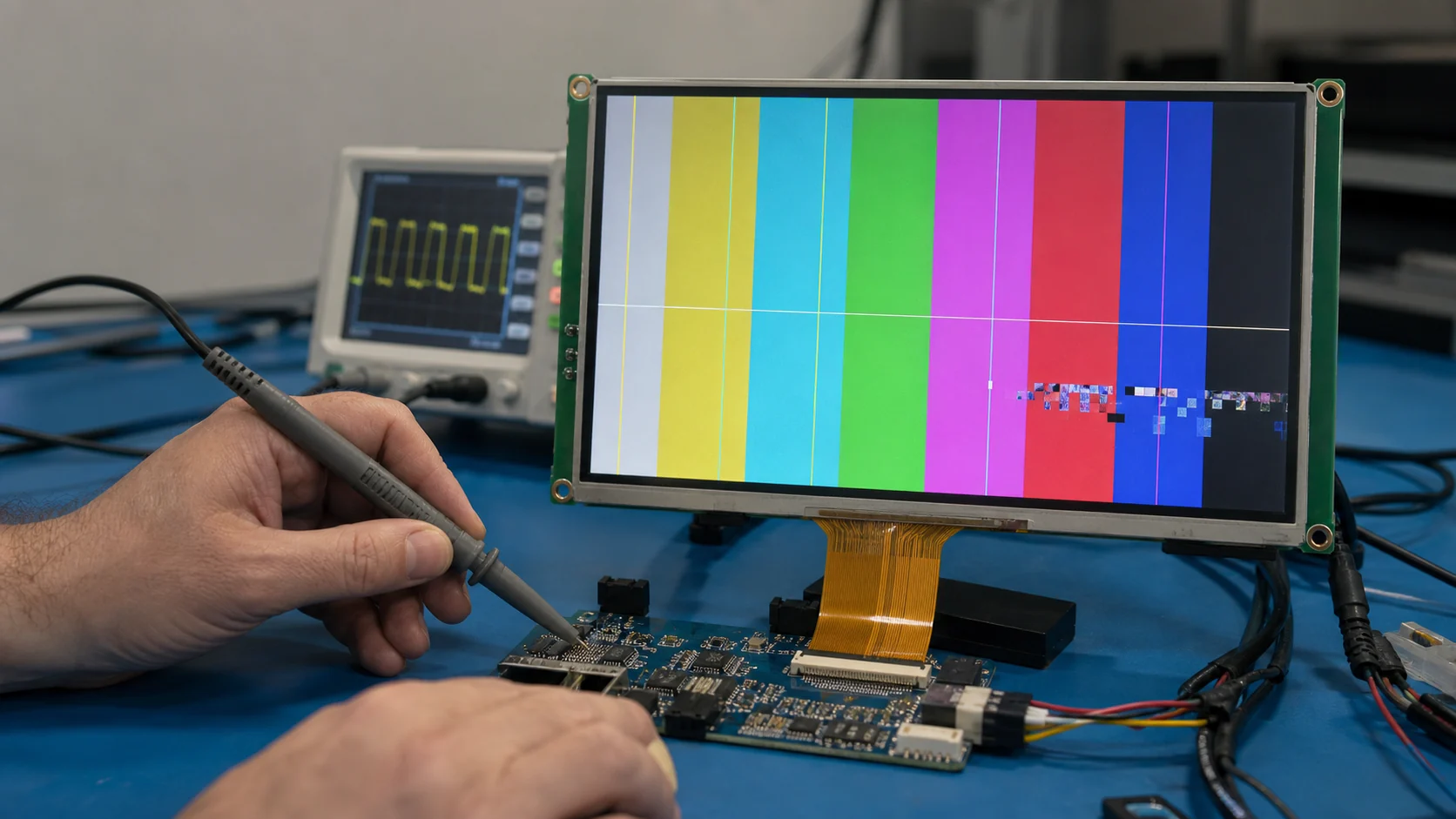
Vertical lines, horizontal lines, random pixels, shifted images, and repeating artifacts on a TFT LCD come from four main areas: corrupted pixel data, incorrect interface timing or format, an intermittent electrical path, or a physical panel defect. Start with controlled test patterns, determine whether the defect is fixed to the glass or moves with the image, and then isolate firmware, interface, connector, power, and module one variable at a time.
The shape of an artifact is useful evidence, but it is not proof by itself. A vertical line can come from a source-driver bond or from a missing data bit. A horizontal line can come from a gate-driver fault or a framebuffer stride error. The diagnostic method below turns the visible pattern into electrical tests.
Classify the Artifact Before Changing Anything
Photograph the screen with a static test pattern and record whether the artifact:
- Stays at the same physical row or column.
- Moves when the image moves.
- Appears only on certain colors or gray levels.
- Changes when the FPC is touched.
- Changes with pixel clock, refresh rate, or interface speed.
- Appears during radio transmission, motor operation, charging, or backlight PWM.
- Worsens with temperature or time.
- Affects every module or only one sample.
Use fixed exposure and avoid camera rolling-shutter bands. A camera artifact can look like an LCD line even when the screen appears clean to the eye.
Symptom-to-Cause Matrix
| Visible symptom | Likely areas | Best first test |
|---|---|---|
| One permanent vertical line | Column driver, glass bond, one FPC path | Solid colors and known-good panel |
| One permanent horizontal line | Gate driver, glass bond, row addressing | Rotate content and compare physical position |
| Multiple evenly spaced lines | Data-bit mapping, stride, lane error | Walking-bit and checkerboard patterns |
| Image shifted left/right | Porch, HSYNC/DE timing, address window | Datasheet timing and active-width check |
| Image shifted up/down | Vertical porch/sync, row offset | Vertical totals and start-address check |
| Random colored speckles | Signal integrity, EMI, clock margin, memory | Reduce interface speed and correlate with noise source |
| Repeating blocks or tearing-like bands | DMA/cache/stride, incomplete transfer | Framebuffer integrity and buffer synchronization |
| Artifacts only on gradients | Color depth, pixel packing, gamma/dither | Solid channel ramps and format check |
| Defect changes when cable moves | FPC/connector/contact | Power off, reseat, inspect, continuity compare |
If the panel is entirely white, use TFT LCD white-screen troubleshooting. If geometry is correct but colors are wrong, use the wrong or inverted TFT colors guide.
Step 1: Use Diagnostic Test Patterns
Application screens hide the structure of a fault. Replace them with patterns that isolate individual paths:
- Solid black, white, red, green, and blue.
- 50% gray and smooth grayscale ramp.
- One-pixel vertical black/white stripes.
- One-pixel horizontal black/white stripes.
- Checkerboard and color bars.
- Walking single bits through each color channel.
- A numbered grid generated in the framebuffer.
Interpretation examples:
- A line visible on every solid color at the same physical coordinate points toward the panel, its driver, or the connection.
- A missing red contribution only when a particular bit is set points toward pixel format, data mapping, or one bus line.
- A repeated pattern every 2, 4, or 8 pixels suggests packing, stride, byte-order, or bus-width alignment.
- A correct framebuffer dump with a bad screen moves attention downstream to the controller, interface, connector, or panel.
Step 2: Decide Whether the Defect Is Fixed to the Panel
Move a sharp graphic across the screen or rotate the content in software.
- If the defect remains on the same physical glass row/column, suspect panel drive, FPC, bonding, or local pressure.
- If it moves with the graphic, suspect framebuffer content, rendering, stride, color conversion, or image assets.
- If it appears only during animation, suspect bandwidth, cache, DMA, tearing, or signal margin.
Do not press hard on the glass. Lightly changing FPC position is a diagnostic clue; applying force to the display can create pressure mura or extend a crack.
Step 3: Verify Framebuffer Address, Stride, and Cache
For systems with a framebuffer, confirm:
- Base address alignment and valid memory range.
- Bytes per pixel and line stride/pitch.
- Horizontal and vertical resolution used by the controller.
- Layer window coordinates and cropping.
- DMA source/destination width and burst settings.
- Cache clean/invalidate operations on cached memory.
- No overlap with stack, heap, camera, or other DMA buffers.
A stride smaller than the real line length wraps pixels into the next row. A stride larger than expected inserts gaps or shifts. Cache incoherency can make old and new blocks appear together even when CPU memory reads seem correct.
Freeze animation and calculate a checksum of each framebuffer line. If corruption already exists in memory, the panel is not the source.
Step 4: Check Pixel Format and Data Mapping
Match the entire path:
graphics format → framebuffer layout → display controller format → physical bus/lane mapping → panel pixel order
Confirm RGB565/RGB666/RGB888, endian/byte order, RGB versus BGR, and the connection of the most-significant bits. On reduced-width RGB buses, suppliers may expect specific upper bits rather than arbitrary truncation.
Use walking-bit colors. If one bit produces no visible change, trace that bit from memory format through the peripheral pin to the module connector. The RGB interface guide provides background on the parallel signal set.
Step 5: Audit Timing and Polarity
For parallel RGB, compare pixel clock, HSYNC, VSYNC, DE, front porch, back porch, pulse width, active size, and polarity with the exact panel datasheet. Confirm totals, not just active resolution.
Measure at the module connector. Wrong or marginal timing may cause:
- Stable image offset.
- Missing first or last rows/columns.
- Periodic line displacement.
- Noise that increases with clock frequency.
- A correct image at one temperature but not another.
Start from supplier typical values. Reduce clock rate within the panel’s allowed range and see whether errors fall sharply. Improvement indicates timing or signal-integrity margin, not a final fix.
For SPI/MCU panels, verify address-window boundaries, transaction byte count, clock mode, write strobe, chip-select behavior, and maximum interface frequency.
For MIPI DSI, review ECC/CRC and PHY error registers, lane count, mode, packet timing, and blanking. See the MIPI DSI debug checklist for the complete sequence.
Step 6: Inspect Signal Integrity and EMI
Random or activity-dependent artifacts deserve a correlation test. Capture the screen while switching one potential aggressor at a time:
- Backlight PWM and boost converter.
- Motors, relays, heaters, or solenoids.
- Wi-Fi, cellular, Bluetooth, or other radios.
- USB or mains charger connection.
- High-current LEDs and GPIO loads.
Inspect clock/data routing, return paths, connector ground pins, cable length, series damping resistors, differential pair geometry, and crosstalk. Probe with suitable bandwidth and a short ground connection; a long oscilloscope ground lead can manufacture ringing that is not present at the receiver.
If a slower edge or lower clock within specification removes errors, review the physical path. If the artifact aligns with system noise, use the practices in EMI testing for embedded displays.
Step 7: Check Power and Ground
Measure logic and analog rails during the artifact. Ripple or transient droop can disturb driver references without turning the display fully off.
Check:
- Module-side logic supply.
- Analog/gate rails if exposed.
- Ground difference between host and display.
- Reset and enable pins near noise events.
- Backlight current transitions.
- Decoupling placement and connector ground continuity.
Artifacts that change with brightness may come from backlight power coupling into LCD rails or shared ground impedance.
Step 8: Inspect Mechanical Stress, FPC, and Connector
Power off and inspect for incomplete insertion, contact contamination, bent pins, cracked solder joints, and FPC creases. Confirm contact side and connector lock.
Mechanical pressure from a bezel, screw, adhesive thickness, or warped enclosure can distort the cell or damage edge bonds. Test the module outside the housing on a supported surface. If the artifact disappears, fix the enclosure stack rather than replacing firmware.
The FPC layout and pin-mapping guide covers contact orientation, grouping, ground returns, and strain relief.
Step 9: Use Known-Good Substitution
Run the same patterns using:
- Known-good panel on the suspect board.
- Suspect panel on a known-good board.
- Shorter or known-good FPC where applicable.
- Supplier evaluation hardware and reference timing.
- Minimal firmware with cache and acceleration simplified.
Change one variable per test. If all panels show the same artifact, investigate the board or software. If one panel alone retains a fixed physical line, document the module lot and return it for failure analysis.
When a Fixed Line Is Probably a Panel Defect
A panel defect is likely when all of the following are true:
- The line remains at the same physical coordinate for every pattern.
- It does not change with clock, interface speed, cable position, or firmware.
- Rails and signals meet specification.
- Another panel works on the same board.
- The suspect panel fails on known-good hardware.
Typical internal mechanisms include source/gate driver failure, chip-on-glass bond damage, cracked transparent conductor, or glass-edge stress. These are not field-repairable at product level.
Prevention Checklist
- Store color-bar and walking-bit patterns in diagnostic firmware.
- Review framebuffer stride, cache, and DMA settings as a unit.
- Measure interface signals at the display connector.
- Provide solid return paths and controlled routing for high-speed signals.
- Add FPC strain relief and prevent bezel pressure on the active stack.
- Validate at temperature extremes and maximum system activity.
- Keep known-good modules from approved production lots.
- Record cosmetic/pixel-line acceptance criteria with the supplier.
Engineering References
- STMicroelectronics AN4861: LCD-TFT display controller on STM32 MCUs — timing, pixel formats, framebuffer, bandwidth, and synchronization behavior.
- NXP AN13573: i.MX 8/RT MIPI DSI/CSI-2 — interface clocks, initialization, packet timing, PHY checks, and error-register diagnostics.
Use these as engineering examples and apply the exact host, bridge, driver IC, and panel documentation for the system under test.
Frequently Asked Questions
What causes vertical lines on a TFT LCD?
Vertical lines often point to a column-data problem: a missing or stuck color/data bit, an FPC contact issue, incorrect pixel packing, a source-driver or glass bond fault, or corrupted framebuffer data. A line fixed to one physical column is more likely panel-related than a line that moves with the image.
What causes horizontal lines on a TFT display?
Horizontal lines can result from row/gate-drive faults, incorrect line timing, memory stride errors, power noise, sync problems, or damaged panel bonds. Determine whether the line is fixed to the glass, tied to particular image content, or changes with clock and temperature.
How do I distinguish a panel fault from a signal problem?
Display solid colors, checkerboards, gradients, and single-pixel patterns, then test a known-good panel and board. A defect that stays at the same physical location on one module across sources suggests the panel. A defect shared by multiple panels or dependent on data, clock, or cable position suggests the board, interface, or firmware.
Can EMI create lines or artifacts on an LCD?
Yes. Coupling into pixel clock, sync, data, reset, power, or touch lines can cause intermittent speckles, shifted pixels, false transitions, or display resets. Correlation with motors, radios, chargers, PWM edges, or cable position is a strong clue.
Can a loose FPC cause only one line on the screen?
It can, especially when a fine-pitch contact carries a specific data bit or control signal. However, a single permanent line can also come from the LCD source/gate driver or a glass bond. Reseat and inspect the FPC before classifying the panel as defective.