
AVDD, VGH, VGL, VCOM: TFT LCD Power Rails Explained
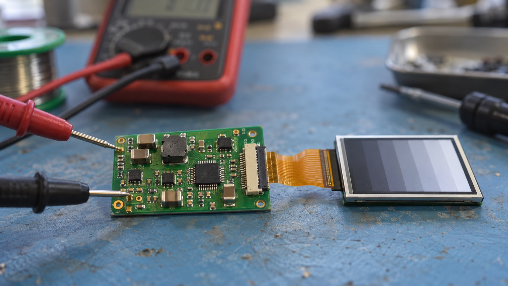
AVDD powers analog pixel-driving circuitry; VGH and VGL provide gate-on and gate-off bias; VCOM establishes the common-electrode reference. These rails help the TFT matrix write and hold pixel voltages. They are different from the digital logic supply and the LED backlight circuit, and their values must come from the exact module specification.
This article explains the functions and a practical measurement workflow. It does not prescribe universal voltages or claim measurements from a particular customer panel. The hero image is an AI-generated electronics illustration.
The Five Power Functions to Keep Separate
| Function | Common label | Purpose | Frequent misunderstanding |
|---|---|---|---|
| Logic and interface power | VDD, IOVCC | Digital control and input thresholds | A 3.3 V supply means every pin tolerates 3.3 V |
| Source-driver analog supply | AVDD, VAA, VS | Supports analog data voltages | It is the same as LED boost voltage |
| Gate-on bias | VGH, VON | Enables selected TFT rows | Higher is always better |
| Gate-off bias | VGL, VOFF | Keeps unselected TFTs off | A negative rail is optional |
| Common-electrode drive | VCOM | Reference for voltage across the liquid crystal | It always equals half of AVDD |
The LED backlight is an additional power function. Its driver regulates current through LED strings and can operate while the LCD’s bias rails are wrong or absent. That is one reason a bright white screen does not establish that the panel electronics are working.
AVDD: Supplying the Analog Data Path
The source drivers convert image data into voltages applied to pixel columns. AVDD supplies the analog circuitry that produces these levels, often together with gamma references and internal regulation.
Insufficient AVDD, excessive ripple, or poor settling can disturb gray levels and image stability. The exact symptom depends on the driver and panel architecture; a washed-out image alone is not enough to identify AVDD as the cause.
Measure AVDD under the specified display patterns and operating conditions. A no-load measurement on a disconnected board cannot prove that the converter remains regulated with the panel scanning. Also inspect voltage drop through connectors, filters, and protection components.
VGH and VGL: Selecting and Isolating Rows
VGH and VGL refer to the high and low gate-driving levels in many TFT architectures. A selected row’s transistors must turn on sufficiently to transfer the source voltage; unselected rows must remain off so pixel charge is retained.
The positive and negative levels are part of a complete panel-driving scheme. Their relationship to the source voltages, transistor characteristics, and timing matters more than their names alone. Changing one voltage can affect stress, leakage, and image behavior elsewhere.
The TI TPS65150 datasheet illustrates one common implementation: a main boost output, positive and negative charge-pump functions, a VCOM buffer, and configurable sequencing. It is an architecture example; the display determines the required operating points.
Gate-drive rails may have relatively small average current but demanding transient behavior. Select the regulator using the required load waveform, output capacitance, startup behavior, and protection response, rather than only an average-current figure.
VCOM: A Reference, Not a Brightness Knob
The liquid crystal responds to the voltage difference between the pixel electrode and the common electrode. LCD driving uses polarity management to avoid an unwanted sustained DC component across the liquid-crystal cell.
VCOM participates in that balance. Its behavior may be a buffered DC level or part of a more complex drive arrangement, depending on the display. A multimeter reports an average and may hide ripple or modulation.
An incorrect VCOM setting can contribute to flicker or image retention, but the same symptoms can come from other causes. Follow the supplier’s adjustment method, test patterns, temperature conditions, and allowed range. Some modules are calibrated at the factory and provide no host-accessible adjustment.
Do not tune VCOM until an image merely looks brighter. First establish correct supplies, pixel format, timing, and gamma configuration. The existing flicker troubleshooting guide helps separate backlight modulation from image-driving problems.
Determine Whether Bias Is Internal or External
The connector specification is the deciding document. A small module with integrated drivers may create all analog and gate bias internally from a single input supply. A different module may expose several required rails, test-only pads, or outputs that must never be driven externally.
For example, the Newhaven NHD-4.3-480272EF-ASXN-T specification identifies the module’s connector assignments and distinguishes its power and backlight connections. Read those assignments before designing an external bias circuit.
For every named net, establish whether it is an input, output, reference, feedback node, or test point. A label on an FPC does not establish that the host should source power into it. The datasheet reading guide provides a broader checklist for resolving these ambiguities.
Build a Rail Measurement Sheet
Use a separate row for every rail required by the approved design:
| Field | What to record |
|---|---|
| Specification | Minimum, typical, maximum, and conditions |
| Ownership | Host-generated, module-generated, or reference output |
| Test location | Connector pin or approved test point and ground reference |
| Startup | Ramp, overshoot, sequencing interval, and settling |
| Running behavior | DC value, ripple, load step, and temperature |
| Shutdown | Discharge time, rail ordering, and residual voltage |
| Result | Measured range, instrument settings, and pass/fail basis |
Do not use absolute maximum ratings as operating targets. They describe stress boundaries, not a region in which correct display operation is guaranteed.
A Step-by-Step Bias Fault Investigation
1. Confirm the Module and Pinout
Compare the physical part label with the drawing and approved sample. Check connector orientation, ground pins, and FPC contact side. Inspect for contamination or a partially latched connector before changing regulator settings.
2. Verify Input Power Under Load
Measure the input at the LCD connector during startup and maximum intended brightness. Shared supplies can droop when the LED driver starts, even if the logic-only load is stable. Record whether the failure begins with illumination, scanout, or a processor load step.
3. Capture Bias Startup Together
Trigger on the enabling event and compare rail ramps with reset and interface activity. Follow the LCD power-sequencing workflow. Correct final voltages do not prove a correct startup sequence.
4. Check Ripple With Suitable Probing
Use a short ground connection and document scope bandwidth. Long ground leads can add apparent ringing. For a negative rail, reference the measurement correctly and use a probe arrangement rated for the circuit; do not attach an earth-referenced ground clip to VGL.
Probe sensitive VCOM or feedback nodes only when permitted and with suitable input impedance. The act of measuring can load a weak reference and change the symptom.
5. Correlate the Fault With Patterns and Temperature
Compare solid fields, gray ramps, and patterns specified by the supplier. Repeat at the intended temperature and supply corners. Keep the interface and firmware constant while investigating bias behavior so several variables do not move at once.
6. Separate Board and Module Causes
Use an approved known-good module or board if available. A rail collapsing only with one panel is evidence to investigate that module or its connection, not immediate proof of a shorted glass assembly. Consider current limiting, sequencing differences, and variant mismatch.
Design Review Questions Before Release
Confirm that every required rail stays in range during load changes and that optional test outputs are not driven by the host. Review converter input limits, charge-pump loading, VCOM stability requirements, capacitor selection, and discharge paths with the component datasheets.
Check layout as well as voltage settings. Keep high-current switching loops and noisy backlight nodes away from sensitive references and touch routing. Retain the actual measurement setup and acceptance limits with the product record so a replacement module or power IC can be qualified against the same evidence.
The useful outcome is a verified relationship between rail function, specified limits, and measured behavior. A list of guessed “typical TFT voltages” cannot provide that relationship.
Frequently Asked Questions
What are AVDD, VGH, VGL, and VCOM in a TFT LCD?
AVDD usually supplies the analog source-driver circuitry, VGH is the gate-on bias, VGL is the gate-off bias, and VCOM drives the common electrode. Exact names, levels, and generation methods depend on the panel.
Are VGH and VGL always supplied by the host board?
No. Many complete display modules generate gate and analog bias internally. Supply external rails only when the module pinout and electrical specification require them.
Is VCOM simply half of AVDD?
No. VCOM is chosen for the panel's driving scheme and electro-optical behavior. It may be generated or adjusted internally, and its approved setting is not determined by a universal half-AVDD rule.
Can a missing VGL rail cause display problems even when the backlight works?
Yes. Incorrect gate-off bias can disrupt pixel isolation and scanning. The backlight is a separate light source, so working LEDs do not prove that the LCD bias system is healthy.
Should I raise LCD bias voltage to fix a faint image?
Do not change bias settings without the panel's approved limits and adjustment procedure. First verify the specified rails, timing, pixel data, gamma settings, and backlight current. Excessive bias can damage the display.